US 11,843,051 B2
Field effect transistor including multiple aspect trapping ratio structures
Mirco Cantoro, Suwon-si (KR); and Yeoncheol Heo, Suwon-si (KR)
Assigned to SAMSUNG ELECTRONICS CO., LTD., Suwon-si (KR)
Filed by SAMSUNG ELECTRONICS CO., LTD., Suwon-si (KR)
Filed on Jul. 8, 2022, as Appl. No. 17/860,820.
Application 17/860,820 is a continuation of application No. 16/923,389, filed on Jul. 8, 2020, granted, now 11,411,111.
Application 16/923,389 is a continuation of application No. 16/211,624, filed on Dec. 6, 2018, granted, now 10,734,521, issued on Aug. 4, 2020.
Application 16/211,624 is a continuation of application No. 15/602,593, filed on May 23, 2017, granted, now 10,181,526, issued on Jan. 15, 2019.
Claims priority of application No. 10-2016-0068928 (KR), filed on Jun. 2, 2016; and application No. 10-2016-0145958 (KR), filed on Nov. 3, 2016.
Prior Publication US 2022/0352375 A1, Nov. 3, 2022
Int. Cl. H01L 29/78 (2006.01); H01L 29/06 (2006.01); H01L 27/088 (2006.01); H01L 29/417 (2006.01); H01L 29/10 (2006.01); H01L 29/66 (2006.01); H01L 21/8238 (2006.01); H01L 21/8234 (2006.01); H01L 21/8258 (2006.01)
CPC H01L 29/7849 (2013.01) [H01L 21/823431 (2013.01); H01L 21/823807 (2013.01); H01L 21/823821 (2013.01); H01L 27/0886 (2013.01); H01L 29/0657 (2013.01); H01L 29/1054 (2013.01); H01L 29/41791 (2013.01); H01L 29/66545 (2013.01); H01L 29/785 (2013.01); H01L 21/8258 (2013.01); H01L 21/823481 (2013.01)] 19 Claims
OG exemplary drawing
 
1. A method of fabricating a field-effect transistor, comprising:
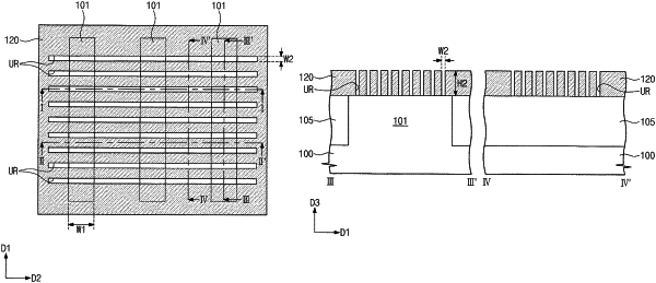
forming a device isolation layer, the device isolation layer including a lower trench that extends in a first direction and exposes a portion of a semiconductor substrate;
forming a mask pattern on the device isolation layer, the mask pattern having upper trenches crossing the lower trench and extending in a second direction that is different from the first direction; and
forming an epitaxial layer in the lower trench and the upper trenches, wherein the epitaxial layer comprises a semiconductor material having a lattice constant is different from that of the semiconductor substrate, and wherein the epitaxial layer includes a lower portion in the lower trench and upper portions in the upper trenches.