| CPC H01L 29/7813 (2013.01) [H01L 29/0634 (2013.01); H01L 29/32 (2013.01); H01L 29/66734 (2013.01)] | 6 Claims |

|
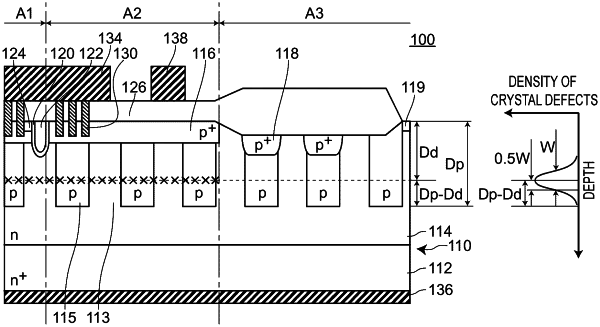
1. A method of manufacturing a MOSFET comprising:
preparing a predetermined structural body, the predetermined structural body including:
a semiconductor base substrate having an n-type column region and a p-type column region, the n-type column region and the p-type column region forming a super junction structure; and
a gate electrode formed on a first main surface side of the semiconductor base substrate by way of a gate insulation film; and
forming a crystal defect in the semiconductor base substrate, wherein
assuming (1) a region of the semiconductor base substrate configured to provide a main operation of the MOSFET when the semiconductor base substrate is completed as the MOSFET as an active region, (2) a region of the semiconductor base substrate disposed on an outer peripheral side of the active region and maintaining a withstand voltage of the MOSFET as an outer peripheral region, and (3) a region of the semiconductor base substrate disposed between the active region and the outer peripheral region as an active connecting region,
in the forming of the crystal defect, out of the active region, the active connecting region, and the outer peripheral region of the semiconductor base substrate, the crystal defects are formed only in the active region and the active connecting region, wherein
the preparing of the predetermined structural body includes forming the semiconductor base substrate and forming the gate electrode in this order, and
the crystal defect is formed after the forming of the gate electrode.
|