| CPC H01L 29/7395 (2013.01) [H01L 27/0255 (2013.01); H01L 27/0727 (2013.01); H01L 29/04 (2013.01); H01L 29/083 (2013.01); H01L 29/1095 (2013.01); H01L 29/32 (2013.01); H01L 29/36 (2013.01); H01L 29/423 (2013.01); H01L 29/66348 (2013.01); H01L 29/7397 (2013.01); H01L 29/8083 (2013.01); H01L 29/861 (2013.01); H01L 29/0834 (2013.01); H01L 29/16 (2013.01); H01L 29/66325 (2013.01); H01L 29/7393 (2013.01); H01L 29/7398 (2013.01); H01L 29/7428 (2013.01); H01L 2924/13055 (2013.01)] | 20 Claims |

|
1. A method of processing an overvoltage protection power semiconductor chip, comprising:
providing a semiconductor body to be coupled to a first load terminal and a second load terminal of the overvoltage protection power semiconductor chip, the first load terminal to be arranged at a frontside and the second load terminal to be arranged at a backside of the overvoltage protection power semiconductor chip, and wherein the semiconductor body comprises each of an active region and an inactive edge region that surrounds the active region,
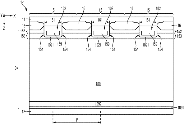
forming, in the active region a plurality of breakthrough cells, each breakthrough cell comprising an insulation structure arranged at the frontside and having a recess into which the first load terminal is to extend and to interface with the semiconductor body;
forming a drift region having dopants of a first conductivity type;
forming an anode region having dopants of a second conductivity type, the anode region being electrically connected to the first load terminal and disposed in contact with the first load terminal;
forming a first barrier region having dopants of the second conductivity type at a lower dopant concentration than the anode region and arranged in contact with each of the anode region and the insulation structure, wherein the first barrier region forms a contiguous semiconductor layer throughout the plurality of breakthrough cells;
forming a second barrier region having dopants of the first conductivity type at a higher dopant concentration than the drift region and separating each of the anode region and at least a part of the first barrier region from the drift region; and
forming a doped contact region arranged in contact with the second load terminal, wherein the drift region is positioned between the second barrier region and the doped contact region.
|