| CPC H01L 29/66462 (2013.01) [H01L 21/823462 (2013.01); H01L 29/2003 (2013.01); H01L 29/205 (2013.01); H01L 29/401 (2013.01); H01L 29/41766 (2013.01); H01L 29/7786 (2013.01); H01L 29/7787 (2013.01)] | 33 Claims |

|
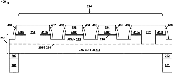
1. A gallium nitride (GaN) based sensor comprising:
a GaN hetero-structure that comprises a GaN layer and a first barrier layer located over the GaN layer, wherein a 2-dimensional electron gas (2DEG) channel is located at an upper surface of the GaN layer, adjacent to the first barrier layer;
a plurality of dielectric structures located over the GaN hetero-structure;
a source contact that extends through a first one of the plurality of dielectric structures and the first barrier layer to contact the 2DEG channel;
a drain contact that extends through a second one of the plurality of dielectric structures and the first barrier layer to contact the 2DEG channel; and
a plurality of gate electrodes that extend over corresponding ones of the plurality of dielectric structures and the 2DEG channel, wherein the gate electrodes are located between the source contact and the drain contact;
wherein the source contact, the drain contact and the gate electrodes have sidewalls that are vertical with respect to an upper surface of the first barrier layer, and each of the plurality of dielectric structures have sidewalls that are sloped at an acute angle with respect to the upper surface of the first barrier layer.
|