| CPC H01L 29/41708 (2013.01) [H01L 29/42304 (2013.01); H01L 29/6681 (2013.01); H01L 29/66234 (2013.01); H01L 29/73 (2013.01); H01L 29/785 (2013.01)] | 20 Claims |

|
1. A method comprising:
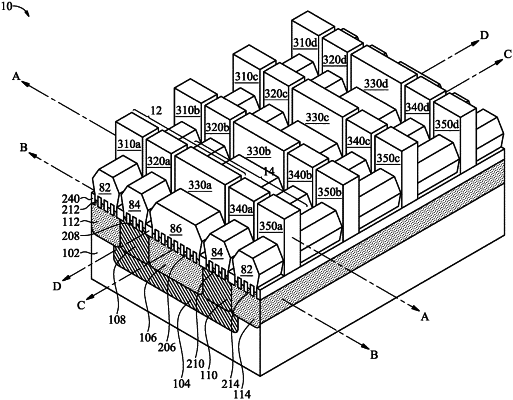
patterning a first doped well of a semiconductor substrate to form first fins, a second doped well of the semiconductor substrate to form second fins, and a third doped well of the semiconductor substrate to form third fins;
forming a gate structure over and along sidewalls of the first fins, the second fins, and the third fins; and
epitaxially growing a first epitaxy of a bipolar junction transistor (BJT) over the first fins on opposing sides of the gate structure, a second epitaxy of the BJT over the second fins on opposing sides of the gate structure, and a third epitaxy of the BJT over the third fins on opposing sides of the gate structure, the first epitaxy and the third conductivity having a first conductivity, the second epitaxy having a second epitaxy opposite the first conductivity, wherein the gate structure has a first portion, a second portion, and a third portion, the first portion, the second portion, and the third portion being electrically separated from each other, the first portion over the first fins, the second portion over the second fins, the third portion over the third fins.
|