| CPC H01L 29/408 (2013.01) [H01L 29/4908 (2013.01); H01L 29/513 (2013.01); H01L 29/6684 (2013.01); H01L 29/7833 (2013.01); H01L 29/78391 (2014.09); H10K 10/474 (2023.02); H01L 29/516 (2013.01)] | 25 Claims |

|
1. A semiconductor device comprising:
a substrate;
a channel layer at least one of on or in the substrate;
an insulation layer on the substrate;
a ferroelectric layer on the insulation layer;
a fixed charge layer on an interface between the insulation layer and the ferroelectric layer, the fixed charge layer including charges of a first polarity; and
a gate on the ferroelectric layer,
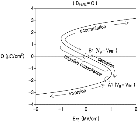
wherein the fixed charge layer is configured to have a charge density that generates a negative capacitance effect in response to the channel layer being in an inversion state, the fixed charge layer having a charge density greater than −5 μC/cm2 and less than 0, or a charge density greater than 0 and less than +5 μC/cm2.
|