| CPC H01L 27/14647 (2013.01) [G02B 5/20 (2013.01); H01L 25/167 (2013.01); H01L 27/1463 (2013.01); H01L 27/1464 (2013.01); H01L 27/14621 (2013.01); H01L 27/14638 (2013.01); H01L 27/14645 (2013.01); H01L 27/14665 (2013.01); H01L 27/14689 (2013.01); H01L 27/14812 (2013.01); H04N 25/00 (2023.01); H01L 27/14612 (2013.01)] | 20 Claims |

|
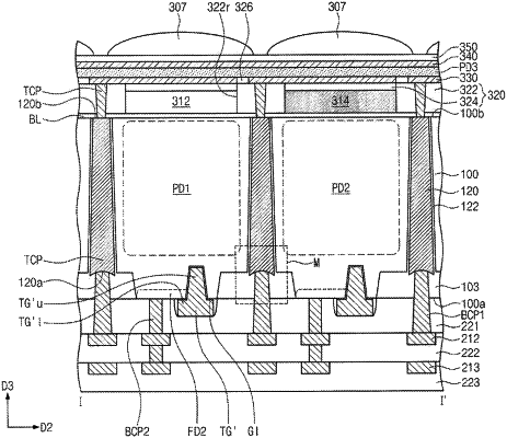
1. An image sensor, comprising:
a substrate having a first surface and a second surface opposite to each other along a first direction;
a first photoelectric conversion region and a second photoelectric conversion region in the substrate;
a first device isolation layer in the substrate, the first device isolation layer having a third surface disposed at the first surface of the substrate, and having a fourth surface disposed at a first distance from the first surface of the substrate;
a through electrode formed along the first direction from the second surface of the substrate, the through electrode having a first end with a non-planar shape adjacent to the fourth surface of the first device isolation layer and a second end adjacent to the second surface of the substrate;
an interlayer dielectric layer on the first surface of the substrate, the interlayer dielectric layer covering the third surface of the first device isolation layer;
a bottom contact plug penetrating the interlayer dielectric layer and the first device isolation layer, the bottom contact plug in contact with the first end of the through electrode;
a transfer gate on the first surface of the substrate, the transfer gate including a first portion within the substrate and a second portion protruding above the first surface of the substrate; and
a photoelectric conversion layer disposed at the second surface of the substrate and electrically connected to the through electrode, wherein:
the first portion of the transfer gate includes a fifth surface disposed at the first surface of the substrate and a sixth surface opposite to the fifth surface,
a center of the first end of the through electrode contacts the bottom contact plug,
a corner of the first end of the through electrode is covered by the first device isolation layer, and
the sixth surface is closer to the second surface of the substrate than the first end of the through electrode.
|