| CPC H01L 27/14636 (2013.01) [H01L 27/1463 (2013.01); H01L 27/14612 (2013.01); H01L 27/14621 (2013.01); H01L 27/14627 (2013.01); H01L 27/14643 (2013.01); H01L 27/14831 (2013.01)] | 17 Claims |

|
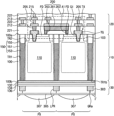
1. An image sensor, comprising:
a substrate having a first surface and a second surface that are opposite to each other, the substrate including a plurality of unit pixel regions having photoelectric conversion regions and floating diffusion regions disposed adjacent to the first surface,
gate electrodes disposed on the first surface of the substrate,
a pixel isolation pattern disposed in the substrate and configured to define the plurality of unit pixel regions; and
an interconnection layer disposed on the first surface of the substrate, the interconnection layer includes a conductive structure,
wherein the conductive structure comprises:
a connection portion that extends parallel to the first surface of the substrate and is spaced apart from the first surface of the substrate, a bottom surface of the connection portion is co-planar with top surfaces of the gate electrodes; and
contacts that extend vertically from the connection portion towards the first surface of the substrate, and
wherein each of the contacts are spaced apart from each other with the pixel isolation pattern interposed therebetween, wherein each of the contacts are coupled to the floating diffusion regions, respectively.
|