| CPC H01L 27/14623 (2013.01) [H01L 27/14625 (2013.01); H01L 27/14638 (2013.01)] | 9 Claims |

|
1. A solid-state imaging device comprising:
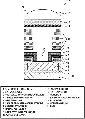
a plurality of pixels arranged in a matrix form on a substrate,
wherein the plurality of pixels each includes
a photoelectric conversion region disposed inside the substrate and configured to convert light entering the substrate into charge,
a charge retaining region disposed more on a side from which the light enters, than the photoelectric conversion region inside the substrate and configured to retain the charge converted in the photoelectric conversion region,
an indented region indented from a surface of the substrate on the side from which the light enters, toward the photoelectric conversion region to at least a depth corresponding to the charge retaining region, and
a light blocking film formed covering the charge retaining region at the surface side of the substrate and extending along a side wall of the indented region.
|