| CPC H01L 27/1461 (2013.01) [G01J 1/44 (2013.01); H01L 27/14634 (2013.01); H01L 31/107 (2013.01); H04N 25/70 (2023.01); G01J 2001/4466 (2013.01)] | 5 Claims |

|
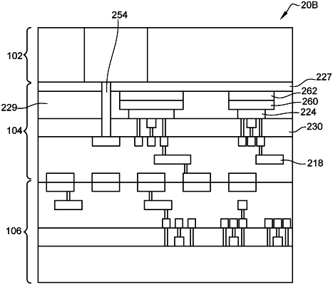
1. A method of manufacturing an electronic device which includes a stack of a first level comprising a SPAD, a second level comprising a quench circuit for said SPAD, and a third level comprising a circuit for processing data generated by said SPAD, the method comprising:
a) forming said first level consisting of a first semiconductor layer including a SPAD and a first insulating layer;
b) forming a stack of layers of the second level comprising a second semiconductor layer, a first interconnection layer including first pads and a second insulating layer;
c) bonding by molecular bonding the second insulating layer of said stack of layers to the first insulating layer of the first level;
d) forming said quench circuit in the second semiconductor layer;
e) forming a stack of layers of the third level comprising a third semiconductor layer and a second interconnection layer including second pads; and
f) bonding by hybrid bonding the first and second interconnection layers and first and second pads.
|