| CPC H01L 27/1203 (2013.01) [H01L 21/02603 (2013.01); H01L 21/84 (2013.01); H01L 27/092 (2013.01); H01L 29/0673 (2013.01); H01L 29/41733 (2013.01); H01L 29/42392 (2013.01); H01L 29/66439 (2013.01); H01L 29/66545 (2013.01); H01L 29/66553 (2013.01); H01L 29/66742 (2013.01); H01L 29/775 (2013.01); H01L 29/78618 (2013.01); H01L 29/78696 (2013.01)] | 20 Claims |

|
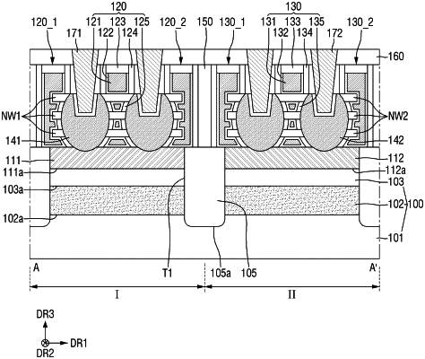
1. A semiconductor device comprising:
a first region including a first lower pattern and a second region adjacent to the first region including a second lower pattern;
a substrate including a first layer, an insulating layer on the first layer, the insulating layer having a first portion and a second portion, and a second layer on the insulating layer;
a first doped layer in the first region and on the second layer extending in a first direction, and including a first impurity;
a second doped layer in the second region and on the second layer, extending in the first direction, and including a second impurity different from the first impurity;
a first plurality of nanowires extending in the first direction on the first doped layer, and sequentially spaced apart from each other in a vertical direction;
a second plurality of nanowires extending in the first direction on the second doped layer and sequentially spaced apart from each other in the vertical direction;
a first gate electrode in a second direction that crosses the first direction, the first gate electrode surrounding the first plurality of nanowires;
a second gate electrode extending in the second direction, the second gate electrode surrounding the second plurality of nanowires; and
an element isolation layer configured to separate the first doped layer from the second doped layer, and contacting the insulating layer,
wherein the first lower pattern includes the first portion of the insulating layer and the second pattern includes the second portion of the insulating layer.
|