| CPC H01L 27/0924 (2013.01) [H01L 23/528 (2013.01); H01L 27/0207 (2013.01); H01L 27/092 (2013.01); H01L 29/785 (2013.01); H03K 3/35625 (2013.01); H03K 3/356156 (2013.01); H03K 19/0948 (2013.01); H03K 19/20 (2013.01); H01L 21/823828 (2013.01); H01L 21/823871 (2013.01)] | 8 Claims |

|
1. A semiconductor device, comprising:
a first inverter configured to receive a first signal, and generate a second signal by inverting the first signal; and
a second inverter configured to receive the second signal, and generate the first signal by inverting the second signal,
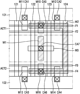
wherein the first inverter includes,
a first active fin extending in a first direction,
a second active fin spaced apart from the first active fin and extending in the first direction,
a third active fin extending in the first direction and being adjacent to the first active fin; and
a fourth active fin spaced apart from the third active fin and being adjacent to the second active fin and extending in the first direction,
a first gate line extending in a second direction, the second direction intersecting the first direction, the first gate line overlapping the first, second, third, and fourth active fins,
a second gate line extending in the second direction and spaced apart from the first gate line, the second gate line overlapping the first and second active fins,
a first metal line electrically connecting the first and second gate lines, the first metal line configured to provide the first signal to both the first gate line and the second gate line,
a second metal line electrically connected to a part of the first active fin between the first gate line and the second gate line and a part of the second active fin between the first gate line and the second gate line, the second metal line configured to transmit the second signal in response to the first signal, and
a third gate line disposed to overlap the first, the second, the third, and the fourth active fins, and spaced apart from the first gate line, the second gate line, and the first metal line.
|