| CPC H01L 25/50 (2013.01) [H01L 21/56 (2013.01); H01L 21/561 (2013.01); H01L 23/552 (2013.01); H01L 24/17 (2013.01); H01L 24/83 (2013.01); H01L 25/0652 (2013.01); H01L 25/16 (2013.01); H01L 23/3128 (2013.01); H01L 23/49816 (2013.01); H01L 23/50 (2013.01); H01L 23/5385 (2013.01); H01L 24/16 (2013.01); H01L 24/81 (2013.01); H01L 24/97 (2013.01); H01L 2224/0401 (2013.01); H01L 2224/05111 (2013.01); H01L 2224/05124 (2013.01); H01L 2224/05139 (2013.01); H01L 2224/05144 (2013.01); H01L 2224/05147 (2013.01); H01L 2224/05155 (2013.01); H01L 2224/1146 (2013.01); H01L 2224/11334 (2013.01); H01L 2224/13023 (2013.01); H01L 2224/13111 (2013.01); H01L 2224/13113 (2013.01); H01L 2224/13116 (2013.01); H01L 2224/13124 (2013.01); H01L 2224/13139 (2013.01); H01L 2224/13144 (2013.01); H01L 2224/13147 (2013.01); H01L 2224/13155 (2013.01); H01L 2224/16235 (2013.01); H01L 2224/16237 (2013.01); H01L 2224/16238 (2013.01); H01L 2224/48091 (2013.01); H01L 2224/48179 (2013.01); H01L 2224/73265 (2013.01); H01L 2224/81815 (2013.01); H01L 2224/97 (2013.01); H01L 2924/15151 (2013.01); H01L 2924/15311 (2013.01); H01L 2924/19105 (2013.01); H01L 2924/19106 (2013.01); H01L 2924/3025 (2013.01)] | 21 Claims |

|
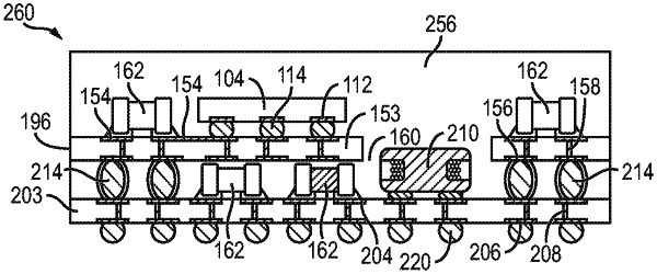
1. A method of making a semiconductor device, comprising:
providing a first substrate;
disposing a first electrical component over the first substrate with a first terminal of the first electrical component oriented toward the first substrate and a second terminal of the first electrical component oriented away from the first substrate, wherein the first electrical component is a discrete active or passive device;
disposing a first solder material between the first terminal of the first electrical component and the first substrate;
disposing a second substrate over the first substrate with the first electrical component between the first substrate and second substrate;
disposing a second solder material between the second terminal of the first electrical component and the second substrate; and
depositing an encapsulant between the first substrate and second substrate and around the first electrical component.
|