| CPC H01L 25/18 (2013.01) [H01L 24/83 (2013.01); H01L 25/50 (2013.01); H10B 12/036 (2023.02); H10B 12/33 (2023.02); H10B 12/482 (2023.02); H10B 12/485 (2023.02); H10B 12/488 (2023.02); H01L 2224/83895 (2013.01); H01L 2224/83896 (2013.01)] | 10 Claims |

|
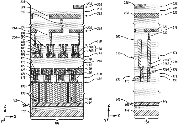
1. A microelectronic device, comprising:
array regions individually comprising:
memory cells comprising access devices and storage node devices;
digit lines coupled to the access devices and extending in a first direction;
word lines coupled to the access devices and extending in a second direction orthogonal to the first direction; and
control logic devices over and in electrical communication with the memory cells;
digit line exit regions horizontally alternating with the array regions in the first direction and individually comprising:
portions of the digit lines extending beyond the array regions adjacent thereto;
digit line contact structures extending through at least some of the portions of the digit lines;
contact structures on the digit line contact structures and individually comprising:
a horizontal pad region comprising a first portion of a conductive material; and
a vertical contact region continuously vertically extending from the horizontal pad region to a position overlying the control logic devices of the array regions, the vertical contact region having smaller horizontal dimensions than the horizontal pad region and comprising a first additional portion of the conductive material integral and continuous with the first portion of the conductive material of the horizontal pad region; and
routing structures coupled to the contact structures; and
word line exit regions horizontally alternating with the array regions in the second direction and individually comprising:
portions of the word lines extending beyond the array regions adjacent thereto;
word line contact structures extending through at least some of the portions of the word lines;
additional contact structures on the word line contact structures and individually comprising:
an additional horizontal pad region comprising a second portion of the conductive material; and
an additional vertical contact region continuously vertically extending from the additional horizontal pad region to the position overlying the control logic devices of the array regions, the additional vertical contact region having smaller horizontal dimensions than the additional horizontal pad region and comprising a second additional portion of the conductive material integral and continuous with the second portion of a conductive material of the additional horizontal pad region; and
additional routing structures coupled to the additional contact structures.
|