| CPC H01L 25/167 (2013.01) [H01L 25/0753 (2013.01); H01L 33/62 (2013.01); H01L 2933/0066 (2013.01)] | 12 Claims |

|
1. A display device comprising:
a substrate;
a pixel circuit layer comprising a plurality of transistors on the substrate;
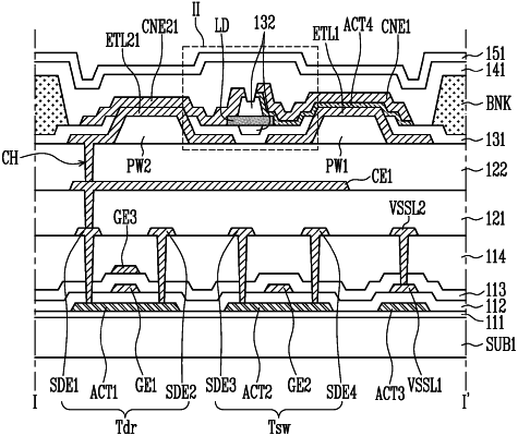
a first partition wall and a second partition wall on the pixel circuit layer, each of the first and second partition walls having a shape protruding in a thickness direction of the substrate;
a first electrode and a second electrode on the same layer and respectively on the first partition wall and the second partition wall;
a light emitting element between the first electrode and the second electrode, the light emitting element comprising:
a first layer comprising a first-type semiconductor material at a first end of the light emitting element;
a second layer comprising a second-type semiconductor material different from the first-type semiconductor material at a second end of the light emitting element; and
an active layer between the first layer and the second layer;
an insulating layer on the light emitting element;
a semiconductor pattern directly on the first electrode and directly contacting the first end of the light emitting element exposed by the insulating layer;
a first contact electrode on the first partition wall and directly on and entirely covering the semiconductor pattern; and
a second contact electrode directly contacting the second end of the light emitting element exposed by the insulating layer,
wherein the semiconductor pattern and the first electrode are between the first contact electrode and the first partition wall in the thickness direction of the substrate,
wherein the semiconductor pattern comprises one of InAIGaN, GaN, AlGaN, InGaN, AIN, and InN.
|