| CPC H01L 25/0652 (2013.01) [H01L 25/50 (2013.01); H01L 2225/06562 (2013.01); H01L 2225/06582 (2013.01); H01L 2225/06593 (2013.01)] | 20 Claims |

|
1. A semiconductor structure, comprising:
a plurality of first dies in a first level;
a plurality of second dies disposed in a second level over each of the first dies; and
a dielectric material surrounding the plurality of first dies and the plurality of second dies,
wherein each of the second dies in the second level overlaps a portion of each of the first dies in the first level.
|
|
6. A semiconductor structure, comprising:
a first die and a second die in a first level;
a third die and a fourth die in a second level over the first level; and
a dielectric material surrounding the first die, the second die, the third die and the fourth die,
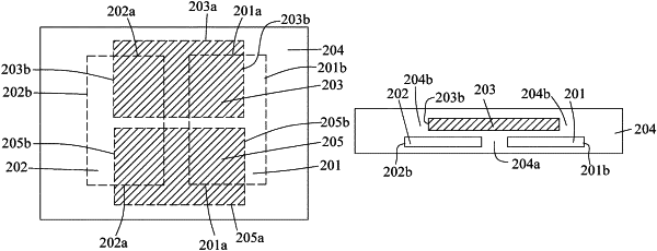
wherein the third die overlaps a portion of the second die and exposes a first corner, a second corner and a third corner of the second die, and the fourth die overlaps a portion of the first die and exposes a first corner, a second corner and a third corner of the first die.
|
|
14. A semiconductor structure, comprising:
a first die and a second die in a first level;
a third die and a fourth die in a second level over the first level;
a dielectric material surrounding the first die, the second die, the third die and the fourth die,
wherein the third die overlaps a portion of the first die and a portion of the second die, and the fourth die overlaps another portion of the first die and another portion of the second die.
|