| CPC H01L 25/0652 (2013.01) [H01L 25/50 (2013.01); H01L 2225/06513 (2013.01); H01L 2225/06541 (2013.01); H01L 2225/06586 (2013.01)] | 17 Claims |

|
1. A semiconductor package, comprising:
an interposer substrate;
outer connection terminals on a bottom surface of the interposer substrate;
chip stacks on the interposer substrate, each of the chip stacks including semiconductor chips and curing layers, which are vertically and alternately stacked; and
a mold layer on the interposer substrate to cover side surfaces of the chip stacks and a top surface of the interposer substrate,
wherein each of the semiconductor chips includes:
a semiconductor substrate,
a penetration structure penetrating the semiconductor substrate,
a circuit insulating layer and interconnection lines on a bottom surface of the semiconductor substrate,
a lower pad connected to the interconnection lines,
an upper pad on the semiconductor substrate, the penetration structure connecting the upper pad to the interconnection lines, and
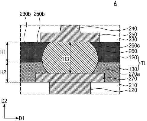
a solder bump on a bottom surface of the lower pad, the solder bump being between the bottom surface of the lower pad and a top surface of the upper pad, and
wherein each of the curing layers includes:
a first curing layer in direct contact with an upper portion of the solder bump of one of the semiconductor chips and in direct contact with only the bottom surface of all surfaces of the lower pad, the first curing layer including a photo-curing agent, and
a second curing layer in direct contact with a lower portion of the solder bump of the one of the semiconductor chips and in direct contact with the top surface of the upper pad, the second curing layer including a thermo-curing agent.
|