| CPC H01L 23/49568 (2013.01) [H01L 21/4842 (2013.01); H01L 21/78 (2013.01); H01L 23/49524 (2013.01); H01L 23/49551 (2013.01); H01L 23/49562 (2013.01); H01L 2224/37147 (2013.01); H01L 2224/38 (2013.01); H01L 2224/40245 (2013.01); H01L 2224/97 (2013.01)] | 8 Claims |

|
1. A method for forming a dual sided chip package comprising:
forming solder on a semiconductor die;
superimposing a frame on the solder over the semiconductor die;
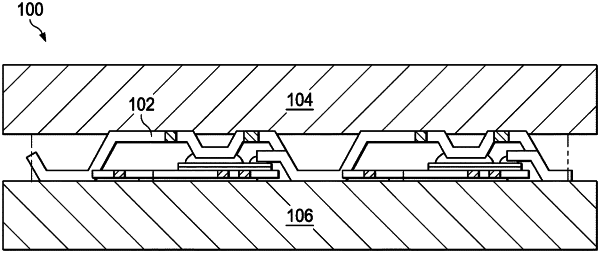
swaging the frame and the semiconductor die between an upside mold die and a downside mold die, wherein:
the frame extends from the upside mold die to the downside mold die; and
the frame is recessed from the upside mold die where the frame contacts the solder over the semiconductor die;
curing the solder;
molding the frame to the semiconductor die with the upside mold die and the downside mold die; and
singulating the frame, wherein heatsink surfaces of the frame are exposed at a first surface of the dual sided chip package and at a second surface of the dual sided chip package, opposite from the first surface.
|