| CPC H01L 23/482 (2013.01) [H01L 21/743 (2013.01); H01L 23/4824 (2013.01); H01L 23/4825 (2013.01); H01L 23/66 (2013.01); H01L 27/0203 (2013.01); H01L 27/0207 (2013.01); H01L 27/1203 (2013.01); H01L 29/1087 (2013.01); H01L 29/41733 (2013.01); H01L 29/78615 (2013.01); H01L 29/78654 (2013.01); H04B 1/40 (2013.01); H01L 21/82385 (2013.01); H01L 21/823456 (2013.01); H01L 2223/6677 (2013.01); H01L 2924/1421 (2013.01)] | 20 Claims |

|
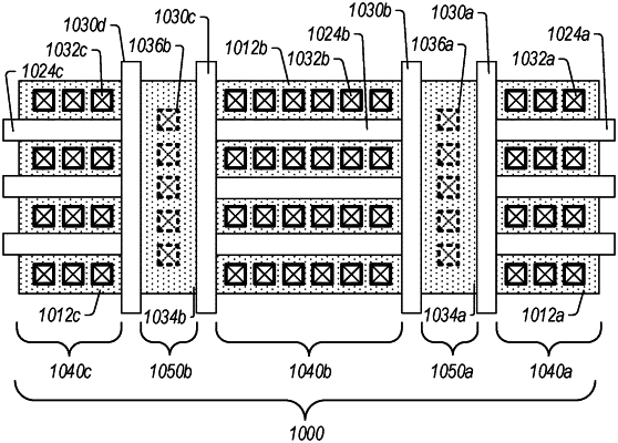
1. A method for fabricating a field-effect transistor (FET), the method comprising:
providing a substrate;
implementing a first assembly of source, gate, and drain on a first active region of the substrate;
implementing a second assembly of source, gate, and drain implemented on a second active region of the substrate;
implementing a third assembly of source, gate, and drain on a third active region of the substrate;
forming a first body contact between the first assembly and the second assembly, the first body contact formed such that application of a voltage on the first body contact influences operation of the first assembly and the second assembly;
forming a second body contact between the second assembly and the third assembly, the first assembly and the third assembly being dimensioned the same such that the first body contact and the second body contact are positioned symmetrically about a center line of the FET, the second assembly being dimensioned such that it has a width that is equal to the combined widths of the first assembly and the third assembly;
forming a finger configuration for the source, the gate, and the drain on each of the first assembly and the second assembly, each finger configuration including a plurality of fingers, the finger configuration of each of the first assembly and the second assembly resulting in source fingers and drain fingers being interleaved with the gate fingers, the source fingers and the drain fingers arranged in alternating rows; and
electrically connecting a particular source finger of the first assembly to a source finger of the second assembly that is positioned on the same row as the particular source finger of the first assembly.
|