| CPC H01L 23/3735 (2013.01) [H01L 23/3733 (2013.01); H01L 23/3737 (2013.01); H01L 23/4985 (2013.01); H01L 25/18 (2013.01); H05K 1/0204 (2013.01); H05K 1/189 (2013.01); H01L 24/16 (2013.01); H01L 24/73 (2013.01); H01L 2224/16227 (2013.01); H01L 2224/73204 (2013.01); H05K 1/147 (2013.01); H05K 2201/10128 (2013.01)] | 15 Claims |

|
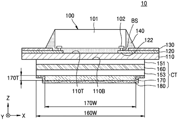
1. A chip-on-film package comprising:
a base film comprising an upper surface and a lower surface opposite to the upper surface;
a semiconductor chip mounted on the upper surface of the base film;
a heat emission layer disposed on the lower surface of the base film to at least partially overlap the semiconductor chip in a thickness direction, wherein the heat emission layer is contiguously formed;
an insulating layer disposed on a lower surface of the heat emission layer; and
a protective layer surrounding side and lower surfaces of the insulating layer.
|