| CPC H01L 23/367 (2013.01) [H01L 23/3677 (2013.01); H01L 23/3736 (2013.01); H01L 23/3738 (2013.01); H01L 23/40 (2013.01); H01L 23/492 (2013.01); H01L 24/19 (2013.01); H01L 25/105 (2013.01); H01L 23/49816 (2013.01); H01L 23/5389 (2013.01); H01L 2224/04105 (2013.01); H01L 2224/12105 (2013.01); H01L 2224/16225 (2013.01); H01L 2224/19 (2013.01); H01L 2224/73259 (2013.01); H01L 2924/15153 (2013.01)] | 9 Claims |

|
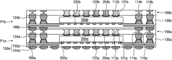
1. A semiconductor package structure, comprising:
a first package structure comprising:
a first redistribution structure comprising metallization patterns and dielectric layers;
a first die over and electrically connected to the first redistribution structure, an active side of the first die comprising contact pads facing the first redistribution structure, and an inactive side of the first die comprising a joining pattern and a solder bump joined to the joining pattern on the first die;
a second die over the first die;
a first connecting plug adjacent the first die and the second die, the first connecting plug electrically connected to the first redistribution structure;
an encapsulant laterally encapsulating the first die, the second die, and the first connecting plug; and
thermal elements on a back-side of the second die;
a second redistribution structure over the back side of the second die and the first connecting plug, the second redistribution structure comprising metallization patterns and a dielectric layer, the second redistribution structure being electrically connected to the first connecting plug; and
a second package structure bonded to the metallization patterns of the second redistribution structure with a first set of conductive connectors.
|