| CPC H01G 4/30 (2013.01) [C04B 35/4682 (2013.01); H01G 4/012 (2013.01); H01G 4/1209 (2013.01); H01G 4/1227 (2013.01); C04B 2235/65 (2013.01)] | 14 Claims |

|
1. A method of manufacturing a ceramic electronic component, the method comprising:
preparing a base material powder having a core-shell structure having a core and a shell, wherein the shell includes a rare earth element R1;
adding a minor component including a rare earth element R2, which is different from the rare earth element R1, to the base material powder to prepare a ceramic green sheet;
printing a conductive paste for an internal electrode on the ceramic green sheet, and then laminating the printed ceramic green sheet to prepare a laminate;
sintering the laminate to prepare a body including a dielectric layer and an internal electrode; and
forming an external electrode on the body,
wherein a content of R2 is 0.1 to 3.0 times a content of R1,
the dielectric layer includes a plurality of dielectric grains,
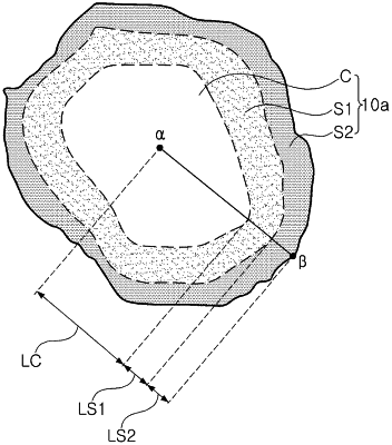
at least one of the plurality of dielectric grains has a core-dual shell structure having a core and a dual shell,
the dual shell includes a first shell surrounding at least a portion of the core, and a second shell surrounding at least a portion of the first shell,
the dual shell includes at least two different types of rare earth elements R1 and R2, and
R2S1/R1S1 is 0.01 or less, R2S2/R1S1 is 0.5 to 3.0, and R1S2/R1S1 is 0.1 to 1.3, where R1S1 and R1S2 denote concentrations of R1 included in the first shell and the second shell, respectively, and R2S1 and R2S2 denote concentrations of R2 included in the first shell and the second shell, respectively, and
a distance corresponding to a thickness of the second shell along a straight line connecting α and β is greater than 4% to less than 25% of a distance between α and β, where a denotes a center of the core-dual shell structure in the cross-section of the core-dual shell structure, and β denotes a point on a surface of the second shell, farthest from α.
|