| CPC G11C 7/1039 (2013.01) [G11C 7/1048 (2013.01); G11C 7/1057 (2013.01); G11C 7/1084 (2013.01); G11C 7/12 (2013.01)] | 20 Claims |

|
1. A memory device comprising:
a memory cell area including a plurality of memory cells and a first metal pad; and
a periphery circuit area comprising a second metal pad, the periphery circuit area vertically connected to the memory cell area via the first metal pad and the second metal pad,
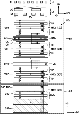
wherein the periphery circuit area further comprises a page buffer circuit comprising:
a plurality of page buffer units in a first horizontal direction, the plurality of page buffer units being connected to the memory cells via a plurality of bit lines; and
a plurality of cache latches in the first horizontal direction, the plurality of cache latches corresponding to each of the plurality of page buffer units and connected to a combined sensing node,
wherein each of the plurality of page buffer units comprises a pass transistor connected to a sensing node of each of the plurality of page buffer units, the sensing node electrically connected to a corresponding bit line, and
wherein the sensing nodes included in the plurality of page buffer units and the combined sensing node are electrically connected to each other through the pass transistors included in the plurality of page buffer units.
|