| CPC G11C 16/24 (2013.01) [G11C 11/5628 (2013.01); G11C 11/5671 (2013.01); G11C 16/10 (2013.01); G11C 16/3459 (2013.01)] | 18 Claims |

|
1. A page buffer, comprising:
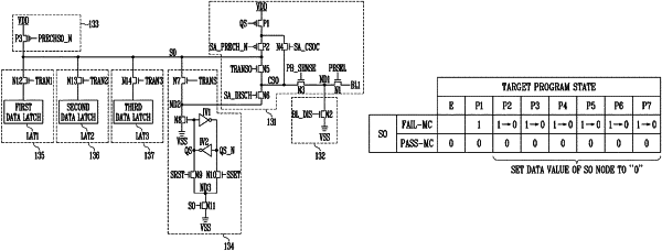
a plurality of data latch components coupled to a sensing node, the plurality of data latch components configured to store program data;
a bit line controller coupled between a bit line and the sensing node, the bit line controller configured to control a node value of the sensing node based on a program state of a memory cell that is coupled to the bit line during a present program verify operation which is being performed; and
a sub-latch component configured to latch verification data indicating a result of the present program verify operation based on the node value of the sensing node,
wherein each of the plurality of data latch components sets the node value of the sensing node to a first logic value based on the program data after controlling the node value of the sensing node, in response that a threshold voltage distribution of a target program state of the memory cell is higher than a threshold voltage distribution of a program state corresponding to the present program verify operation, and
wherein the target program state corresponds to the program data.
|