| CPC G09G 3/3648 (2013.01) [G02F 1/1368 (2013.01); G09G 3/3696 (2013.01); G09G 2300/0426 (2013.01); G09G 2330/021 (2013.01)] | 5 Claims |

|
1. A display apparatus comprising:
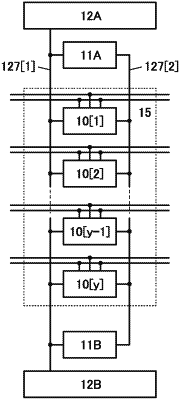
a first circuit configured to output first data;
a second circuit configured to generate second data by inverting the first data;
a third circuit configured to output third data;
a fourth circuit configured to generate fourth data by inverting the third data; and
a display region comprising a pixel,
wherein the first circuit is positioned on one end side of the display region,
wherein the third circuit is positioned on the other end side of the display region,
wherein the pixel comprises a first transistor, a second transistor, a third transistor, a first capacitor, and a fifth circuit which comprises a display device,
wherein one of a source and a drain of the first transistor is electrically connected to one electrode of the first capacitor and the third circuit,
wherein one of a source and a drain of the second transistor is electrically connected to one of a source and a drain of the third transistor and the other electrode of the first capacitor,
wherein the other of the source and the drain of the first transistor and the other of the source and the drain of the second transistor are electrically connected to at least one of the first circuit and the third circuit, and
wherein the other of the source and the drain of the third transistor is electrically connected to at least one of the second circuit and the fourth circuit.
|