| CPC G09G 3/3266 (2013.01) [G09G 3/32 (2013.01); G09G 3/3233 (2013.01); G09G 3/3241 (2013.01); G09G 3/3275 (2013.01); G09G 3/3677 (2013.01); G09G 2300/0408 (2013.01); G09G 2300/0426 (2013.01); G09G 2300/0439 (2013.01); G09G 2300/0809 (2013.01); G09G 2300/0819 (2013.01); G09G 2300/0861 (2013.01); G09G 2310/0202 (2013.01); G09G 2310/0216 (2013.01); G09G 2310/0218 (2013.01); G09G 2310/0251 (2013.01); G09G 2310/0262 (2013.01); G09G 2310/0286 (2013.01); G09G 2310/08 (2013.01); G09G 2320/0223 (2013.01); G09G 2320/045 (2013.01); G09G 2340/0435 (2013.01)] | 17 Claims |

|
1. A display device, comprising:
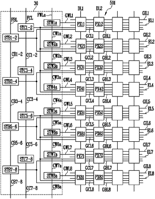
a plurality of compensation stages connected to a plurality of compensation scan lines, each of the plurality of compensation scan lines connected to different pixel rows; and
a plurality of pixels, each of the plurality of pixels comprising a first transistor including a first electrode, a second electrode, and a gate electrode and a third transistor having a first electrode connected to the second electrode of the first transistor, a second electrode connected to the gate electrode of the first transistor, and a gate electrode connected to one of the plurality of compensation scan lines,
wherein the plurality of compensation stages comprises first to fourth compensation stages,
wherein the first compensation stage has an output terminal connected to P (an integer larger than 1) of the plurality of compensation scan lines,
wherein the second compensation stage is connected to the first compensation stage through a first compensation carry line and has no compensation scan line connected thereto,
wherein the third compensation stage is connected to the second compensation stage through a second compensation carry line and has an output terminal connected to Q (an integer larger than C) and smaller than P) of the plurality of compensation scan lines,
wherein the fourth compensation stage is connected to the third compensation stage through a third compensation carry line and has an output terminal connected to R (an integer the same as Q) of the plurality of compensation scan lines, and
wherein a number of pixels connected to each of P of the plurality of compensation scan lines is less than a number of pixels connected to each of Q of the plurality of compensation scan lines.
|