| CPC G09G 3/3266 (2013.01) [G09G 3/3225 (2013.01); G09G 2310/0264 (2013.01); G09G 2310/08 (2013.01); G09G 2330/021 (2013.01)] | 18 Claims |

|
1. A scan driver comprising:
a driving circuit, the driving circuit including:
a control circuit configured to output a first control signal to a first node and a second control signal to a second node in response to a clock signal and a carry signal, and
an output circuit connected between a first voltage terminal to which a first voltage is supplied and a second voltage terminal to which a second voltage is supplied, and configured to output a first scan signal to a first output terminal in response to the first control signal and the second control signal; and
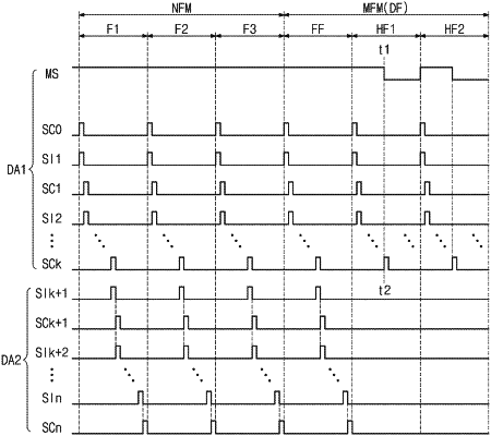
a masking circuit configured to receive the first control signal and the second control signal and output a second scan signal to a second output terminal in response to the first control signal and the second control signal, the masking circuit being connected to an input terminal to which a masking signal is supplied and configured to control the voltage level of the second scan signal in accordance with the masking signal,
wherein the masking circuit and the output circuit are connected in common to the first voltage terminal or the second voltage terminal, and
wherein the masking signal has a first level and is deactivated in a normal frequency mode, and the masking signal comprises an inactive period having the first level and an active period having a second level in a multi-frequency mode.
|