| CPC G09G 3/3233 (2013.01) [H01L 25/0753 (2013.01); H01L 25/167 (2013.01); H01L 33/0095 (2013.01); H01L 33/20 (2013.01); H01L 33/38 (2013.01); H01L 33/44 (2013.01); H01L 33/52 (2013.01); H05B 45/40 (2020.01); H01L 33/62 (2013.01)] | 15 Claims |

|
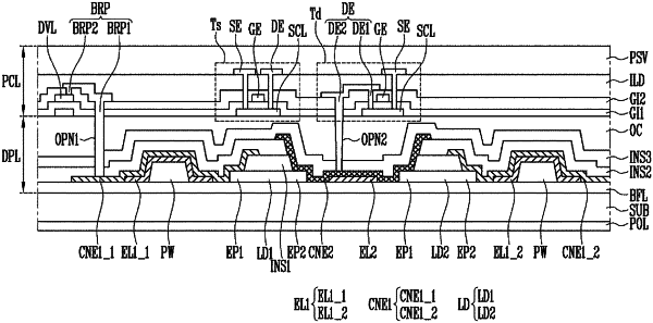
1. A display device comprising:
a pixel configured to emit light of a first color in a display area, the pixel comprising:
a substrate;
a light emitting element on one surface of the substrate and configured to emit the light of the first color, the light emitting element having a lower surface adjacent to the substrate and an upper surface facing the lower surface in a thickness direction of the substrate;
a first electrode on the one surface of the substrate, on the upper surface of the light emitting element, and electrically connected to one end of the light emitting element;
a second electrode on the one surface of the substrate, on the upper surface of the light emitting element, and electrically connected to another end of the light emitting element;
an insulation layer on the first electrode, the second electrode, and the upper surface of the light emitting element, the insulation layer having a first opening exposing a portion of the second electrode; and
a transistor on the insulation layer and electrically connected to the light emitting element,
wherein the insulation layer is between the upper surface of the light emitting element and the transistor, and
wherein the second electrode is electrically connected to the transistor through the first opening.
|