| CPC G09G 3/3225 (2013.01) [H10K 50/86 (2023.02); H10K 50/865 (2023.02); H10K 59/131 (2023.02); H10K 59/38 (2023.02); H10K 59/40 (2023.02); G06F 3/013 (2013.01); G06F 3/02 (2013.01); G06F 3/03545 (2013.01); G06F 3/041 (2013.01); G09G 3/2007 (2013.01); G09G 2300/0426 (2013.01); G09G 2300/0439 (2013.01); G09G 2310/0286 (2013.01); G09G 2310/08 (2013.01); G09G 2320/0233 (2013.01); G09G 2320/0247 (2013.01); G09G 2330/021 (2013.01); G09G 2354/00 (2013.01)] | 10 Claims |

|
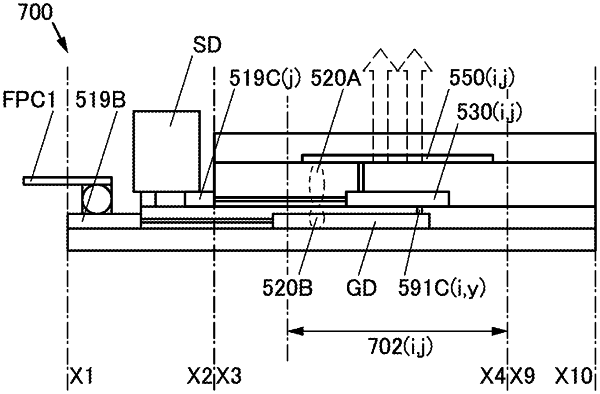
1. A display panel comprising:
a display region;
a first functional layer; and
a second functional layer comprising a first opening portion,
wherein the display region comprises a pixel,
wherein the pixel comprises a display element and a pixel circuit,
wherein the first functional layer comprises the pixel circuit and a scan line,
wherein the display element is electrically connected to the pixel circuit,
wherein the pixel circuit is electrically connected to the scan line,
wherein the second functional layer comprises a region overlapping with the first functional layer,
wherein the second functional layer comprises a driver circuit and a wiring,
wherein the driver circuit is provided so that the pixel circuit is positioned between the driver circuit and the display element,
wherein the wiring is electrically connected to the scan line at the first opening portion, and
wherein the wiring is electrically connected to the driver circuit.
|