| CPC G09G 3/32 (2013.01) [G09G 2300/0426 (2013.01); G09G 2300/0452 (2013.01); G09G 2300/0842 (2013.01); G09G 2310/0278 (2013.01); G09G 2320/0271 (2013.01); G09G 2320/043 (2013.01); G09G 2320/045 (2013.01)] | 20 Claims |

|
1. A display device, comprising:
a display panel comprising a plurality of pixels; and
a driving circuit configured to receive an image signal and provide a data signal to the plurality of pixels such that an image is displayed on the display panel,
wherein:
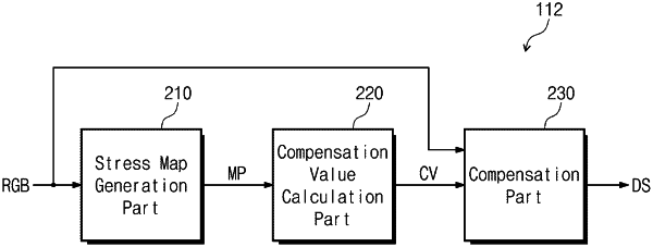
the driving circuit comprises:
a stress map generator configured to divide the image signal into a plurality of blocks and generate a stress map having a representative value of each of the plurality of blocks;
a compensation value calculator configured to calculate a compensation value corresponding to each of the plurality of pixels based on the stress map; and
a compensator configured to output the data signal obtained by compensating the image signal based on the compensation value when a gray scale level of the image signal is less than or equal to a reference gray scale level;
the plurality of pixels comprise first color subpixels, second color subpixels, and third color subpixels, and
a compensation value corresponding to each of the first color subpixels, the second color subpixels, and the third color subpixels is set to a representative value of a first block among the plurality of blocks, when the image signal corresponding to each of the first color subpixels in the first block corresponds to a maximum gray scale level and when the image signal corresponding to each of the second color subpixels and the third color subpixels in the first block corresponds to a minimum gray scale level.
|