US 11,841,814 B2
System with cache-coherent memory and server-linking switch
Krishna Teja Malladi, San Jose, CA (US); Andrew Chang, Los Altos, CA (US); and Ehsan M. Najafabadi, San Jose, CA (US)
Assigned to Samsung Electronics Co., Ltd., Yongin-si (KR)
Filed by Samsung Electronics Co., Ltd., Suwon-si (KR)
Filed on Aug. 12, 2022, as Appl. No. 17/887,379.
Application 17/887,379 is a continuation of application No. 17/026,074, filed on Sep. 18, 2020, granted, now 11,416,431.
Claims priority of provisional application 63/031,508, filed on May 28, 2020.
Claims priority of provisional application 63/031,509, filed on May 28, 2020.
Claims priority of provisional application 63/068,054, filed on Aug. 20, 2020.
Claims priority of provisional application 63/057,746, filed on Jul. 28, 2020.
Claims priority of provisional application 63/006,073, filed on Apr. 6, 2020.
Prior Publication US 2022/0382702 A1, Dec. 1, 2022
This patent is subject to a terminal disclaimer.
Int. Cl. G06F 13/40 (2006.01); G06F 3/06 (2006.01); G06F 9/4401 (2018.01); G06F 12/0802 (2016.01); G06F 12/0808 (2016.01); G06F 12/1045 (2016.01); G06F 13/16 (2006.01); G06F 15/173 (2006.01); G06F 13/42 (2006.01); G06F 13/28 (2006.01); H04L 49/45 (2022.01); H04L 49/351 (2022.01)
CPC G06F 13/4027 (2013.01) [G06F 3/0604 (2013.01); G06F 3/067 (2013.01); G06F 3/0619 (2013.01); G06F 3/0625 (2013.01); G06F 3/0629 (2013.01); G06F 3/0647 (2013.01); G06F 3/0653 (2013.01); G06F 3/0659 (2013.01); G06F 3/0679 (2013.01); G06F 9/4401 (2013.01); G06F 12/0802 (2013.01); G06F 12/0808 (2013.01); G06F 12/1045 (2013.01); G06F 13/1663 (2013.01); G06F 13/28 (2013.01); G06F 13/409 (2013.01); G06F 13/4022 (2013.01); G06F 13/4068 (2013.01); G06F 13/4221 (2013.01); G06F 15/17331 (2013.01); H04L 49/45 (2013.01); G06F 2212/621 (2013.01); G06F 2213/0026 (2013.01); G06F 2213/28 (2013.01); H04L 49/351 (2013.01)] 20 Claims
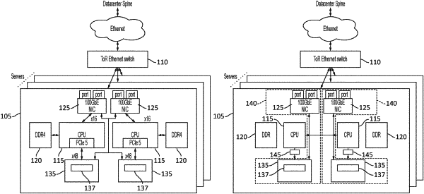
OG exemplary drawing
 
1. A system, comprising:
a first server, comprising:
a processing circuit,
a first switch configured to adhere to a cache coherent protocol, and
a first memory device; and
a second switch connected to the first server,
wherein:
the first memory device is connected to the first switch via a first interface,
the first switch is connected to the second switch, and
the processing circuit is connected to the first switch via a second interface different from the first interface.