| CPC G06F 12/123 (2013.01) [G06F 3/0619 (2013.01); G06F 3/0652 (2013.01); G06F 3/0658 (2013.01); G06F 3/0659 (2013.01); G06F 9/30043 (2013.01); G06F 12/0246 (2013.01); G06F 12/1027 (2013.01); G06F 3/0679 (2013.01)] | 6 Claims |

|
1. A memory controller for controlling a memory device, the memory controller comprising:
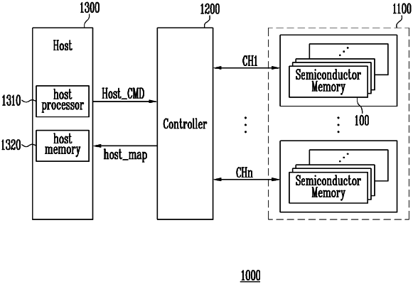
a buffer memory configured to store map data including mapping information of logical addresses of data provided from an external host and physical addresses of memory cells included in the memory device, wherein the physical addresses correspond to the logical addresses, respectively;
a host control circuit configured to provide host map data which includes some of the map data to the external host;
a map data control block configured to:
receive a read request from the external host, and
check a history of the map data transmitted to the external host in order to determine from the history that same map data is stored in both the external host and the buffer memory, wherein the same map data includes target mapping information corresponding to a logical address of the read request; and
a flash control circuit configured to acquire the target mapping information and process the read request according to the target mapping information.
|