| CPC G05F 1/59 (2013.01) | 8 Claims |

|
1. A distributed LDO regulator structure without an external capacitor, at least comprising:
one CORE module; and
a plurality of POWER modules driven by the CORE module;
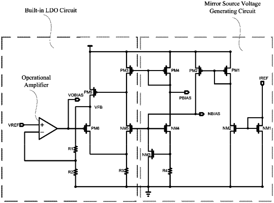
wherein the CORE module comprises a mirror source voltage generating circuit and a built-in LDO regulator circuit;
wherein the mirror source voltage generating circuit comprises:
a first, a second, a third and a fourth NMOSs; and
a first, a second, and a fourth PMOSs;
wherein a gate and a drain of the first NMOS and a gate of the second NMOS are all connected to a current input end IREF;
wherein a drain of the second NMOS, a drain and a gate of the first PMOS, and a gate of the second PMOS are connected to each other; and wherein a source of the fourth NMOS is connected to a gate of the third NMOS;
wherein the built-in LDO regulator circuit comprises:
an operational amplifier;
a third, a fifth, and a sixth PMOSs; and
a fifth NMOS;
wherein an output end of the operational amplifier and a gate of the sixth PMOS together serve as a control voltage end VOBIAS of one of the plurality of POWER modules; wherein respective sources of the fifth PMOS, the third PMOS, the fourth PMOS, the second PMOS, and the first PMOS are connected to each other; wherein a gate of the fifth PMOS, a drain of the third PMOS, and a drain of the fifth NMOS are connected to each other;
wherein a gate of the third PMOS, a drain of the fourth PMOS, and a drain of the fourth NMOS are connected to each other, with a connection end serving as a voltage bias end PBIAS;
wherein a gate of the fifth NMOS, a gate of the fourth NMOS, a drain of the third NMOS, and a drain of the second PMOS are connected to each other, with a connection end serving as a voltage bias end NBIAS; wherein a negative input end of the operational amplifier is connected to a drain of the fifth PMOS and a source of the sixth PMOS by means of a first resistor, with a connection end serving as an output end of the built-in LDO regulator circuit;
wherein said module of the plurality of POWER modules comprises:
a sixth NMOS, a seventh PMOS, an eighth PMOS, and a ninth PMOS;
wherein a drain of the seventh PMOS, a gate of the eighth PMOS, and a drain of the sixth NMOS are connected to each other;
wherein a source of the seventh PMOS and a source of the eighth PMOS are connected to each other;
wherein a drain of the eighth PMOS and a source of the ninth PMOS are connected to each other, with a connection end serving as an output end VOUT of said module of the plurality of POWER modules;
wherein a source of the sixth MOS and a drain of the ninth MOS are connected to each other;
wherein a gate of the seventh PMOS is connected to the voltage bias end PBIAS;
wherein a gate of the sixth NMOS is connected to the voltage bias end NBIAS; and
wherein a gate of the ninth PMOS is connected to the control voltage end VOBIAS.
|