| CPC G02F 1/1368 (2013.01) [G02F 1/133514 (2013.01); G02F 1/134309 (2013.01); G02F 1/136286 (2013.01); H01L 27/1222 (2013.01); G02F 1/13624 (2013.01)] | 12 Claims |

|
1. An array substrate, comprising:
a base substrate; and
a plurality of pixel units disposed on the base substrate in an array, wherein each of the pixel units comprises:
a main pixel electrode;
a sub-pixel electrode;
a first thin film transistor (TFT) electrically connected to the sub-pixel electrode and comprising:
a first source electrode;
a first drain electrode;
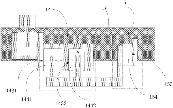
a first channel, wherein at least a portion of the first channel is disposed between the first source electrode and the first drain electrode, and the first channel comprises two or more subchannels; and
a first semiconductor layer comprising two or more semiconductor sublayers, wherein each of the semiconductor sublayers is disposed in a corresponding subchannel;
a second TFT electrically connected to the first TFT and comprising:
a second source electrode;
a second drain electrode;
a second channel disposed between the second source electrode and the second drain electrode; and
a second semiconductor layer disposed in the second channel; and
a third TFT electrically connected to the main pixel electrode;
wherein the first channel comprises a first subchannel and a second subchannel disposed between the first source electrode and the first drain electrode, the first subchannel and the second subchannel are spaced apart from each other, and both the first subchannel and the second subchannel are U-shaped.
|