US 11,841,595 B2
Display device
Masatoshi Yokoyama, Tochigi (JP); Shigeki Komori, Tochigi (JP); Manabu Sato, Tochigi (JP); Kenichi Okazaki, Tochigi (JP); and Shunpei Yamazaki, Setagaya (JP)
Assigned to Semiconductor Energy Laboratory Co., Ltd., Kanagawa-ken (JP)
Filed by Semiconductor Energy Laboratory Co., Ltd., Atsugi (JP)
Filed on Dec. 21, 2022, as Appl. No. 18/085,689.
Application 18/085,689 is a continuation of application No. 17/580,742, filed on Jan. 21, 2022, granted, now 11,543,718.
Application 17/580,742 is a continuation of application No. 17/366,474, filed on Jul. 2, 2021, granted, now 11,327,376, issued on May 10, 2022.
Application 17/366,474 is a continuation of application No. 17/082,094, filed on Oct. 28, 2020, granted, now 11,137,651, issued on Oct. 5, 2021.
Application 17/082,094 is a continuation of application No. 16/865,672, filed on May 4, 2020, granted, now 10,877,338, issued on Dec. 29, 2020.
Application 16/865,672 is a continuation of application No. 16/583,817, filed on Sep. 26, 2019, granted, now 10,852,576, issued on Dec. 1, 2020.
Application 16/583,817 is a continuation of application No. 16/026,227, filed on Jul. 3, 2018, granted, now 10,437,091, issued on Oct. 8, 2019.
Application 16/026,227 is a continuation of application No. 15/144,916, filed on May 3, 2016, granted, now 10,018,887, issued on Jul. 10, 2018.
Application 15/144,916 is a continuation of application No. 14/746,885, filed on Jun. 23, 2015, granted, now 9,366,894, issued on Jun. 14, 2016.
Application 14/746,885 is a continuation of application No. 13/942,468, filed on Jul. 15, 2013, granted, now 9,097,925, issued on Aug. 4, 2015.
Claims priority of application No. 2012-161726 (JP), filed on Jul. 20, 2012.
Prior Publication US 2023/0129465 A1, Apr. 27, 2023
Int. Cl. G02F 1/1362 (2006.01); G02F 1/1333 (2006.01); G02F 1/1343 (2006.01)
CPC G02F 1/136227 (2013.01) [G02F 1/13439 (2013.01); G02F 1/133345 (2013.01); G02F 1/134309 (2013.01); G02F 1/136277 (2013.01); G02F 1/134372 (2021.01); G02F 2202/02 (2013.01); G02F 2202/10 (2013.01)] 3 Claims
OG exemplary drawing
 
3. A display device comprising:
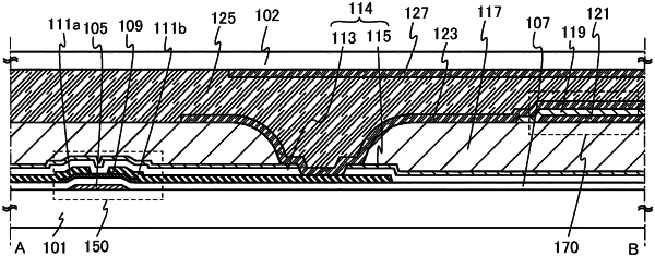
an oxide semiconductor film over a substrate, the oxide semiconductor film comprising at least one of indium, gallium, and zinc;
a first conductive film over the oxide semiconductor film, the first conductive film functioning as one of a source and a drain of a transistor;
a first insulating film over the first conductive film;
a second insulating film over the first insulating film;
a third insulating film over the second insulating film;
a fourth insulating film over the third insulating film;
a second conductive film over the third insulating film;
a third conductive film over the fourth insulating film; and
a liquid crystal layer over the third conductive film,
wherein the third conductive film is electrically connected to the first conductive film via a first opening provided in the first insulating film, a second opening provided in the second insulating film, a third opening provided in the third insulating film, and a fourth opening provided in the fourth insulating film,
wherein the first conductive film, the first insulating film, the second insulating film, the fourth insulating film, and the third conductive film overlap each other in this order,
wherein the first insulating film, the second insulating film, and the fourth insulating film comprise silicon,
wherein the third insulating film comprises an organic material,
wherein the oxide semiconductor film comprises a channel formation region of the transistor, and
wherein the second conductive film and the third conductive film overlap each other with the third insulating film provided therebetween.