| CPC G02B 5/3058 (2013.01) [G01J 3/0224 (2013.01); G02B 26/06 (2013.01); G02B 27/286 (2013.01); G01J 2003/2806 (2013.01); G01J 2003/2826 (2013.01); G02B 5/008 (2013.01); G02B 2207/101 (2013.01)] | 20 Claims |

|
1. A polarizing filter comprising:
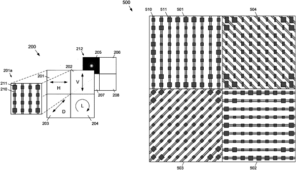
a wire grid comprising multiple wire elements, each wire element being spaced from an adjacent wire element and extending across the polarizing filter along a longitudinal axis of the wire element; and
an array of phase-modulating nanostructures formed on the wire grid, the array of phase-modulating nanostructures changing a phase of incident light a predetermined amount of phase change, each phase-modulating nanostructure being located in the array with respect to a corresponding wire element and in alignment with other phase-modulating nanostructures along the longitudinal axis of the corresponding wire element, each phase-modulating nanostructure comprising a square or a rectangular shape, a first width and a second width, the first width being perpendicular to the second width, and the first width and the second width of each phase-modulating nanostructure varying with respect to the first width and the second width of other phase-modulating nanostructures of the array based on a location of the phase-modulating nanostructure in the array.
|