| CPC B41J 2/3556 (2013.01) | 11 Claims |

|
1. A semiconductor device for controlling energization of a heating element that performs printing, the semiconductor device comprising:
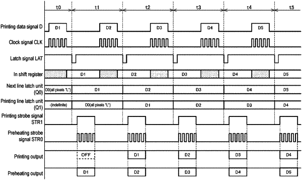
a strobe signal input unit receiving a printing strobe signal that causes the heating element to generate heat for printing;
a preheating strobe generation circuit generating a preheating strobe signal that causes the heating element to preheat by compressing a waveform of the printing strobe signal in a time axis direction; and
an output controller outputting a control signal that controls energization of the heating element based on the printing strobe signal and the preheating strobe signal.
|