| CPC B41J 2/04541 (2013.01) [B41J 2/0455 (2013.01); B41J 2/04581 (2013.01)] | 7 Claims |

|
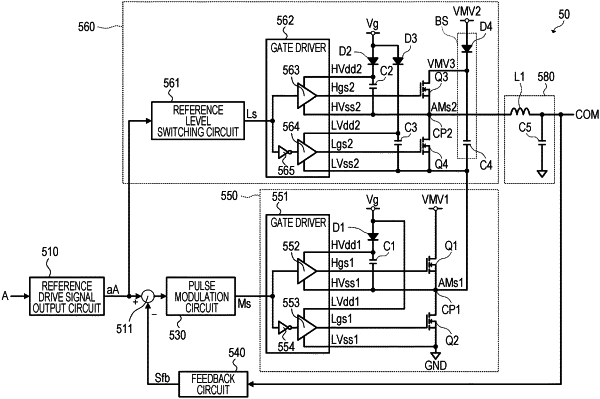
1. A drive circuit that outputs a drive signal driving a drive portion, the circuit comprising:
a modulation circuit that outputs a modulation signal obtained by modulating a reference drive signal which is a reference of the drive signal;
an amplifier circuit that outputs an amplification modulation signal obtained by amplifying the modulation signal from a first output point;
a level shift circuit that outputs a level shift amplification modulation signal obtained by shifting a potential of the amplification modulation signal from a second output point; and
a demodulation circuit that demodulates the level shift amplification modulation signal and outputs the drive signal, wherein
the amplifier circuit includes
a first gate driver that outputs a first gate signal and a second gate signal based on the modulation signal,
a first transistor of which a first voltage is supplied to one end, and the other end is electrically coupled to the first output point, and which operates based on the first gate signal, and
a second transistor of which one end is electrically coupled to the first output point and which operates based on the second gate signal,
the level shift circuit includes
a bootstrap circuit to which a second voltage and the amplification modulation signal are input and that outputs a third voltage,
a second gate driver that outputs a third gate signal and a fourth gate signal based on the reference drive signal,
a third transistor of which the third voltage is supplied to one end, and the other end is electrically coupled to the second output point, and which operates based on the third gate signal, and
a fourth transistor of which one end is electrically coupled to the second output point, and the other end is electrically coupled to the first output point, and which operates based on the fourth gate signal,
a potential of the first voltage is larger than a potential of the second voltage, and
the second gate driver outputs the third gate signal that switches an operation of the third transistor and the fourth gate signal that switches an operation of the fourth transistor, in a period during which a potential of the drive signal is between a potential of the first voltage and a potential of the second voltage.
|