| CPC H01G 4/232 (2013.01) [H01G 2/06 (2013.01); H01G 4/30 (2013.01); H05K 1/185 (2013.01); H01G 4/2325 (2013.01); H05K 2201/10015 (2013.01); Y10T 29/435 (2015.01)] | 20 Claims |

|
1. A multilayer ceramic electronic component to be embedded in a board comprising:
a ceramic body including dielectric layers and having two end surfaces in a length direction, two surfaces in a width direction, and two surfaces in a thickness direction;
first and second internal electrodes formed to be alternately exposed to the two end surfaces of the ceramic body in the length direction, having the dielectric layers interposed therebetween; and
a first external electrode electrically connected to the first internal electrodes and a second external electrode electrically connected to the second internal electrodes, the first and second external electrodes being formed on the two end surfaces of the ceramic body in the length direction,
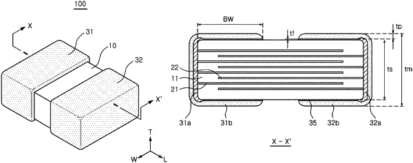
wherein the first and second external electrodes each include first and second base electrodes formed on the two end surfaces of the ceramic body in the length direction, a conductive thin film layer formed on each of [ the ] two surfaces of the ceramic body in the thickness direction, and plating layers formed on the first and second base electrodes and the conductive thin film layers,
the conductive thin film layers of each of the first external electrode or the second external electrode are separate from each other [ ,
an average thickness of the conductive thin film layers is smaller than an average thickness of each of the first and second base electrodes,
when a thickness of the conductive thin film layers is defined as tf and a thickness of the plating layers formed on the conductive thin film layers is defined as tp, 1.5≤tp/tf≤10000 is satisfied, and
when widths of band surfaces of the first and second external electrodes formed on the conductive thin film layers of one surface of the ceramic body in the thickness direction are defined as BW, each of BW is 25% or more of a length of the ceramic body] .
|