| CPC H10K 59/353 (2023.02) [H10K 50/15 (2023.02); H10K 50/16 (2023.02); H10K 50/171 (2023.02); H10K 59/122 (2023.02); H10K 59/131 (2023.02)] | 22 Claims |

|
1. A light emitting display device comprising:
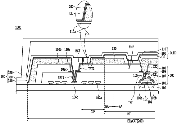
a substrate having an active area and a non-active area surrounding the active area, wherein the non-active area is positioned between the active area and an end line of the substrate;
a plurality of light emitting devices provided in subpixels within the active area;
a voltage line provided within the non-active area along an edge of the active area of the substrate; and
a bank to expose emission parts of the light emitting devices through a plurality of first holes at the active area and to expose the voltage line through a second hole at the non-active area,
wherein an electron injection layer is provided throughout the active area,
wherein the electron injection layer extends to the non-active area to be provided inside the second hole and covers an edge of the bank adjacent to the end line of the substrate, and
wherein the electron injection layer overlaps and entirely covers an exposed surface of the voltage line exposed by the bank in the second hole.
|