| CPC H10K 59/131 (2023.02) [G09G 3/3225 (2013.01); H10K 59/123 (2023.02)] | 20 Claims |

|
1. A display panel, comprising:
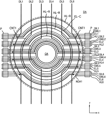
a substrate including a display area surrounding an opening area and a non-display area between the opening area and the display area;
a plurality of display elements in the display area;
a plurality of scan lines extending in a first direction in the display area and detouring around the opening area in the non-display area;
a plurality of data lines extending in a second direction crossing the first direction in the display area, the plurality of data lines detouring around the opening area in the non-display area;
a plurality of voltage lines extending in the second direction in the display area; and
a plurality of electrode voltage lines extending in the first direction in the display area and electrically connected to the plurality of voltage lines, wherein the plurality of voltage lines and the plurality of electrode voltage lines form a mesh structures in a plan view.
|