| CPC H10K 59/122 (2023.02) [H10K 50/822 (2023.02); H10K 59/173 (2023.02)] | 20 Claims |

|
1. A device having a plurality of sub-pixels, each sub-pixel comprising:
a section of a substrate;
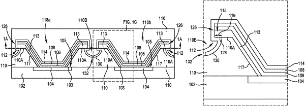
first and second pixel-defining layer (PDL) structures comprising a non-conductive material, each of the first and second PDL structures having a trench disposed between peripheral portions of an upper surface of each of the first and second PDL structures;
first and second inorganic overhangs, each of the first and second inorganic overhangs defined by an overhang extension of an inorganic layer disposed on sidewalls and the peripheral portions of the upper surface of the first and second PDL structures, the overhang extension extending laterally past the trench to define the first and second PDL overhangs;
an anode;
an organic light-emitting diode (OLED) material disposed on the anode, the inorganic layer disposed on the sidewalls and the peripheral portions of the upper surface of the first and second PDL structures, and the overhang extension of the inorganic layer; and
a cathode disposed on the OLED material disposed over:
the anode;
the inorganic layer disposed on the sidewalls and the peripheral portions of the upper surface of the first and second PDL structures; and
the overhang extension of the inorganic layer.
|