| CPC H10K 59/1216 (2023.02) [H10K 50/813 (2023.02); H10K 50/818 (2023.02); H10K 50/852 (2023.02); H10K 50/865 (2023.02); H10K 59/122 (2023.02); H10K 59/38 (2023.02); H10K 2102/3026 (2023.02)] | 16 Claims |

|
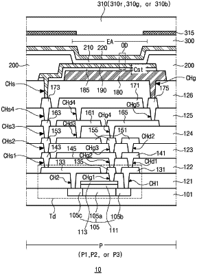
1. An organic light emitting display device, comprising:
a substrate;
a plurality of pixels on the substrate;
a driving transistor including a gate electrode, a source electrode, and a drain electrode;
a reflection electrode on the driving transistor, the reflection electrode electrically connected to the gate electrode of the driving transistor;
a dielectric layer on the reflection electrode;
a first electrode on the dielectric layer and facing the reflection electrode, the first electrode electrically connected to the source electrode of the driving transistor;
an organic light emitting layer on the first electrode; and
a second electrode on the organic light emitting layer,
wherein each of the plurality of pixels includes first, second and third pixel regions displaying first, second and third colors, respectively, wherein the first, second, and third colors are different from each other,
wherein the first color has a wavelength longer than that of the second color, and the second color has a wavelength longer than that of the third color, and
wherein the dielectric layer of the first pixel region has a thickness greater than that of the dielectric layer of the second pixel region, and the dielectric layer of the second pixel region has a thickness greater than that of the dielectric layer of the third pixel region.
|