| CPC H10K 59/1216 (2023.02) [H01L 27/1225 (2013.01); H01L 27/1244 (2013.01); H01L 27/1255 (2013.01); H01L 29/24 (2013.01); H01L 29/66757 (2013.01); H01L 29/7869 (2013.01); H01L 29/78675 (2013.01); H10K 59/123 (2023.02); H10K 59/1213 (2023.02); H10K 59/131 (2023.02)] | 23 Claims |

|
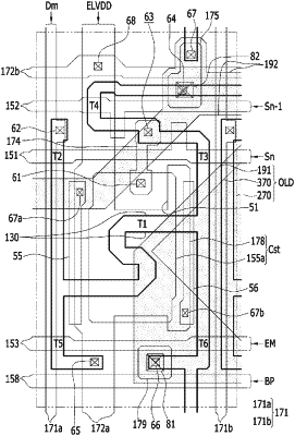
1. An organic light emitting diode display device comprising:
a substrate;
a scan line over the substrate and configured to transmit a scan signal;
a data line crossing the scan line and configured to transmit a data voltage;
a driving voltage line crossing the scan line in a plan view and configured to transmit a driving voltage;
a switching transistor connected to the scan line and the data line;
a driving transistor connected to the switching transistor;
a driving connector connected to a driving gate electrode of the driving transistor;
a storage capacitor comprising a first storage electrode, and a second storage electrode; and
a pixel electrode electrically connected to the driving transistor,
wherein the first storage electrode and the driving connector are connected via a contact hole,
wherein the second storage electrode comprises a curved edge at least partly surrounding the contact hole in the plan view,
wherein the pixel electrode does not overlap the curved edge in the plan view,
wherein the first storage electrode corresponds to the driving gate electrode,
wherein the contact hole does not overlap the pixel electrode, and
wherein the pixel electrode overlaps the second storage electrode, but does not overlap the curved edge in the plan view.
|