| CPC H10K 50/858 (2023.02) [G06F 3/0412 (2013.01); H10K 50/818 (2023.02); H10K 59/122 (2023.02); H10K 59/124 (2023.02); H10K 59/40 (2023.02); G06F 3/0446 (2019.05); G06F 3/04164 (2019.05); G06F 2203/04111 (2013.01); G06F 2203/04112 (2013.01); H10K 50/824 (2023.02); H10K 2102/3026 (2023.02)] | 20 Claims |

|
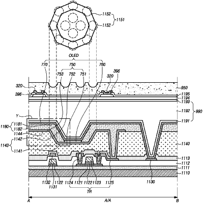
1. A touch display device, comprising:
a substrate including an active area and a non-active area;
a transistor disposed on the substrate;
a sub-pixel electrically connected to the transistor, and including an organic light emitting diode;
an encapsulation layer disposed on the organic light emitting diode;
a planarization layer disposed on the encapsulation layer, and including a lens unit; and
a plurality of touch electrodes disposed between the encapsulation layer and the planarization layer, the plurality of touch electrodes including an open area,
wherein the lens unit is disposed in the open area of the plurality of touch electrodes, and
wherein the sub-pixel includes at least two emission areas and at least one non-emission area in the open area of the plurality of touch electrodes,
the at least one non-emission area being configured to be in a black state or to have a lower brightness than the at least two emission areas of the sub-pixel.
|