US 11,839,105 B2
Display device
Seunghun Kim, Yongin-si (KR); Sooyoun Kim, Yongin-si (KR); Wooyong Sung, Yongin-si (KR); Seungho Yoon, Yongin-si (KR); and Moonwon Chang, Yongin-si (KR)
Assigned to SAMSUNG DISPLAY CO., LTD., Yongin-si (KR)
Filed by SAMSUNG DISPLAY CO., LTD., Yongin-si (KR)
Filed on Oct. 4, 2022, as Appl. No. 17/959,986.
Application 17/959,986 is a continuation of application No. 17/182,120, filed on Feb. 22, 2021, granted, now 11,462,717, issued on Oct. 4, 2022.
Application 17/182,120 is a continuation of application No. 16/418,578, filed on May 21, 2019, granted, now 10,930,885, issued on Feb. 23, 2021.
Claims priority of application No. 10-2018-0075579 (KR), filed on Jun. 29, 2018.
Prior Publication US 2023/0026398 A1, Jan. 26, 2023
This patent is subject to a terminal disclaimer.
Int. Cl. H10K 50/844 (2023.01); H10K 50/84 (2023.01); H10K 50/842 (2023.01); H10K 77/10 (2023.01); H10K 59/131 (2023.01)
CPC H10K 50/844 (2023.02) [H10K 50/84 (2023.02); H10K 50/8426 (2023.02); H10K 77/10 (2023.02); H10K 59/131 (2023.02)] 20 Claims
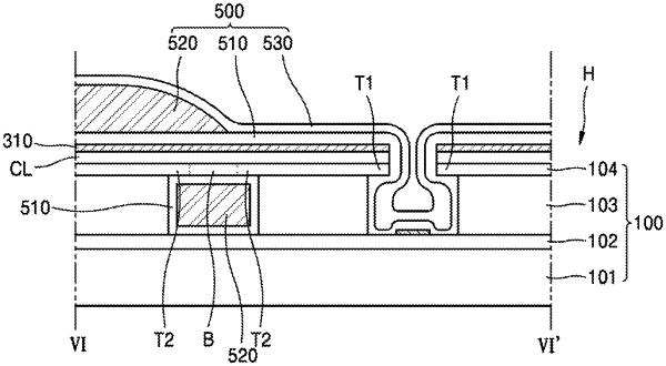
OG exemplary drawing
 
1. A display device, comprising:
a substrate;
a circuit layer on the substrate;
a display element on the circuit layer, wherein the display element includes a first electrode, a second electrode and an intermediate layer between the first electrode and the second electrode;
at least one hole arranged within a display area and that penetrates the substrate;
a first groove arranged between the at least one hole and the display area, and that surrounds the at least one hole;
a second groove arranged between the first groove and the display area and that surrounds the first groove; and
an encapsulation layer that covers the display element,
wherein the encapsulation layer comprises an organic encapsulation layer that fills the second groove.