| CPC H10K 59/121 (2023.02) [H10K 50/86 (2023.02); H10K 59/1315 (2023.02); H10K 59/351 (2023.02); H10K 59/352 (2023.02); H10K 59/65 (2023.02)] | 20 Claims |

|
1. A display substrate comprising a substrate, comprising:
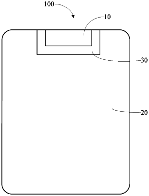
a first display region provided with a plurality of first sub-pixels disposed on the substrate, and each of the plurality of first sub-pixels further comprising:
a first electrode;
a light-emitting structure disposed on the first electrode;
a second electrode disposed on the light-emitting structure;
a second display region provided with a plurality of second sub-pixels disposed on the substrate; and
a third display region provided with a plurality of third sub-pixels disposed on the substrate, the third display region disposed contiguous to both the first display region and the second display region;
wherein a light transmittance of the first display region is greater than a light transmittance of the second display region and a light transmittance of the third display region respectively; a density of the plurality of second sub-pixels is greater than a density of the plurality of third sub-pixels and a density of the plurality of first sub-pixels respectively; and
a pixel circuit for driving the plurality of first sub-pixels is disposed in the third display region, wherein the first electrode of each of the plurality of first sub-pixels is electrically connected to a corresponding pixel circuit via a wiring, and the wiring comprises a first segment and a second segment which are connected with each other, and the first segment is disposed in the first display region, and the second segment is disposed in the third display region, and the first segment is made of a transparent conductive material.
|