| CPC H10B 43/27 (2023.02) [G11C 5/063 (2013.01); H01L 24/09 (2013.01); H01L 25/0657 (2013.01)] | 5 Claims |

|
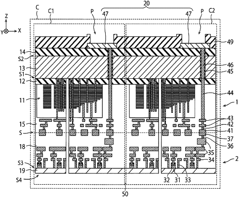
1. A method of manufacturing a semiconductor device, comprising:
forming a first control circuit on a first substrate in a first region of a surface of the first substrate;
forming a first memory cell array electrically connected to the first control circuit, above the first control circuit in the first region;
forming a first pad electrically connected to the first control circuit, above the first memory cell array in the first region;
forming a second control circuit on the first substrate in a second region of the surface of the first substrate;
forming a second memory cell array electrically connected to the second control circuit, above the second control circuit in the second region;
forming a second pad electrically connected to the second control circuit, above the second memory cell array in the second region;
forming a connection line electrically connecting the first pad to the second pad; and
dicing a wafer including the semiconductor device to cut the connection line, thereby manufacturing a semiconductor device including the first control circuit, the first memory cell array and the first pad, and a semiconductor device including the second control circuit, the second memory cell array and the second pad.
|