| CPC H10B 43/20 (2023.02) [H10B 41/10 (2023.02); H10B 41/20 (2023.02); H10B 41/35 (2023.02); H10B 43/10 (2023.02); H10B 43/35 (2023.02)] | 13 Claims |

|
1. A semiconductor memory device comprising:
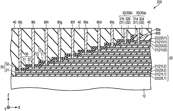
a stacked layer body including a plurality of conductive layers stacked to be apart from each other in a first direction, and including a stair-like end with a plurality of rising parts and a plurality of terrace parts;
a plurality of pillar structures each including a semiconductor layer extending in the first direction through the stacked layer body;
an upper insulating layer provided to cover the stacked layer body including the stair-like end;
a stopper insulating layer provided between the upper insulating layer and the stacked layer body to be disposed along the stair-like end of the stacked layer body; and
a plurality of contacts passing through the upper insulating layer to be connected to the conductive layers, respectively, wherein
the stopper insulating layer does not extend in a second direction perpendicular to the first direction between the upper insulating layer and an uppermost conductive layer of the plurality of conductive layers provided to correspond to a first rising part which is an uppermost one of the rising parts, and the plurality of contacts pass through the stopper insulating layer to be connected to the conductive layers, excluding one contact of the plurality of contacts which is connected to the uppermost conductive layer, wherein
the stacked layer body includes an uppermost insulating layer provided to correspond to the first rising part on the uppermost conductive layer, and the one contact passes through the uppermost insulating layer to be connected to the uppermost conductive layer.
|