| CPC H10B 43/20 (2023.02) [H10B 41/10 (2023.02); H10B 41/20 (2023.02); H10B 41/35 (2023.02); H10B 43/10 (2023.02); H10B 43/27 (2023.02); H10B 43/35 (2023.02)] | 15 Claims |

|
1. A semiconductor storage device, comprising:
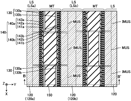
a first conductive layer and a second conductive layer arranged in a first direction;
a plurality of first semiconductor layers facing the first conductive layer, the first semiconductor layers disposed between the first conductive layer and the second conductive layer, the plurality of first semiconductor layers being arranged in a second direction that intersects the first direction;
a first charge storage layer that is disposed between the plurality of first semiconductor layers and the first conductive layer in the first direction, and the first charge storage layer extending in the second direction over a plurality of regions between the plurality of first semiconductor layers and the first conductive layer; and
a first insulating layer disposed between the plurality of first semiconductor layers and the first charge storage layer in the first direction,
wherein the first insulating layer includes:
a first region that faces one end of each of the first semiconductor layers in the second direction, the first region extending in the first direction,
a second region that faces the other end of each of the first semiconductor layers in the second direction, the second region extending in the first direction, and
a third region disposed between the first region and the second region in the second direction; and
the first region and the second region each have a lower nitrogen concentration than the third region,
wherein an end of the first region in the first direction contacts an end of the first semiconductor layer in the first direction.
|